
NEWS
Photon Bridge Bets €10 Million on Weaker AI Lasers
Photon Bridge raised €10 million to multiplex lower-power lasers for 2028 AI optics, a yield bet that now runs beside NVIDIA’s $2 billion Lumentum supply deal.

Photon Bridge raised €10 million (about $11 million) on October 21, 2026 to build multi-wavelength laser sources for AI data centers. Amadeus APEX Technology Fund and 360 Capital co-led the round. Existing backers Innovation Industries, Faber and the Brabant Development Agency (BOM) put in more money after a €4.75 million seed in January 2025.
The Eindhoven company is betting that many lower-power lasers, combined on silicon, can be made in the millions by 2028, the same year NVIDIA has already reserved high-power laser supply.
Investors Are Paying for a Yield Architecture
Omdia forecasts that more than 20 million data-centre AI accelerators will ship each year by 2028. As those clusters grow from thousands of processors toward hundreds of thousands, moving data between chips has become a hard limit on performance, and optical links are moving closer to the package. Co-packaged optics puts the optical engine beside the switch or accelerator. That shift needs a far larger supply of the lasers that generate the light.
Today’s high-power laser chain was built for telecom and subsea networks, where volumes are much lower. Photon Bridge’s pitch is that AI turns the laser into a semiconductor-scale part, so the die itself cannot keep getting harder to make. The company combines and multiplexes light from several lower-power semiconductor lasers rather than driving a few devices to higher power. Lower power density makes each laser less sensitive to defects, which is how it argues yield can hold as volumes rise.
AI is fundamentally changing the way computing infrastructure is built. We are moving towards enormous systems in which hundreds of thousands of processors have to operate together, and moving data between them is becoming one of the defining constraints on performance. That means optics has to move closer to the compute. But it also creates an entirely different manufacturing challenge. The industry will soon need millions of these laser sources every year. Instead of making individual lasers increasingly powerful and difficult to manufacture, we move that scaling challenge into the architecture.
Paul Marchal, CEO, Photon Bridge
Ion Hauer, an investment partner at APEX Ventures, said every new wave of compute creates fresh bottlenecks further down the supply chain, and that lasers are the next one. Cesare Maifredi, a partner at 360 Capital, said AI is turning lasers from a telecom component into a semiconductor-scale product, and that once the talk is millions of units a year, yield becomes fundamental. The new money is meant to speed product work and customer qualification, put first samples in customers’ hands in 2027, and prepare for volume manufacturing from 2028, while the Eindhoven team grows.
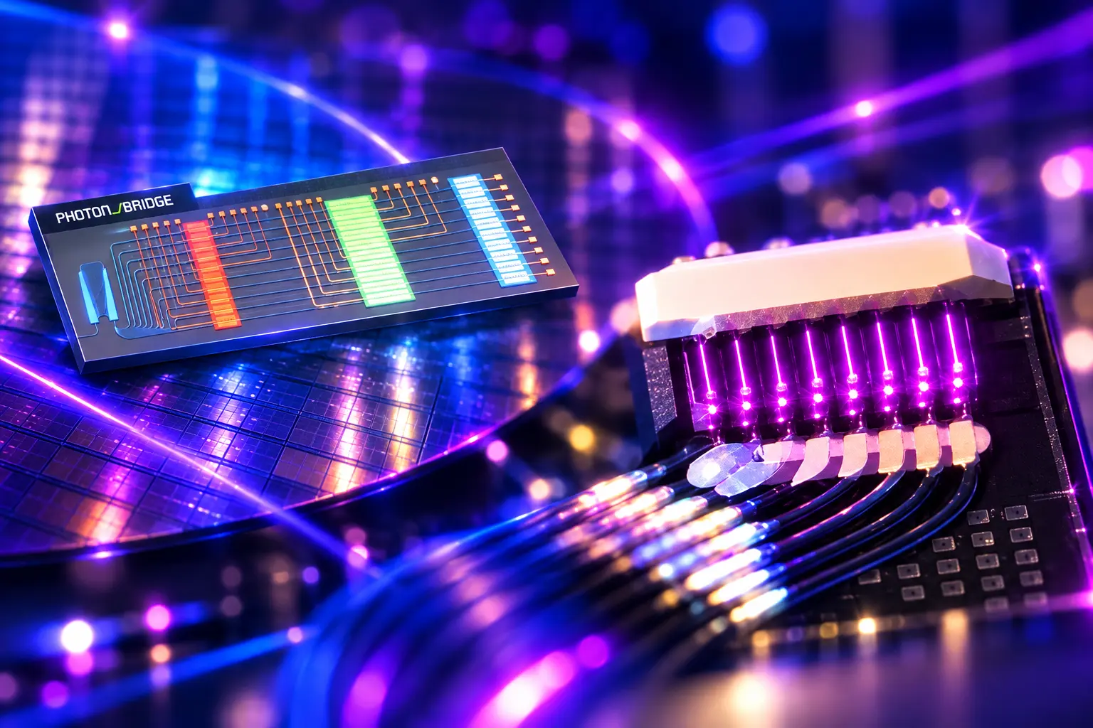
How the Cantilever Turns a 2 µm Bond Into 200 nm
Photon Bridge started in 2020 as Photon IP, founded by Rui Santos, now chief technology officer, and Xaveer Leijtens, an associate professor in photonic integration at Eindhoven University of Technology. Santos had worked on lasers at SMART Photonics and imec. The pair’s claim is that stacking every function in one photonic stack hurts yield. Active parts such as lasers stay in indium phosphide. Passive waveguides sit in silicon. A patented cantilever waveguide is the joint between them.
Standard chip-assembly bonders place parts to about 2 µm. The company says the silicon cantilevers flex during bonding and convert that placement error into passive alignment better than 200 nm at the laser-silicon interface, with no active alignment step. Optical and electrical bonds happen in the same flip-chip pass. Angled facets with anti-reflection coatings are specified for back reflection below -40 dB and link loss under 1 dB.
The silicon is a thick-film platform with 2 µm waveguides, against the 220 nm films common in silicon photonics. Photon Bridge estimates that geometry at about 5 times lower loss, 50 times higher optical power handling, and 25 times less sensitivity to linewidth and etch variation. The laser keeps its gain on the InP die. The silicon takes over only after the facet, so the foundry’s laser design is not rewritten by the attach.
THREE PLATFORM CLAIMS
- Optical power: The October 21 design target is up to 40 mW of optical power per wavelength per fibre, with thick-film guides specified to hold more than 1 W on-chip.
- Channel count: A multiplexer on the silicon interposer beside the laser array is the company’s path to 8, 16 and 32 wavelengths, adding colors instead of raising per-die power.
- A 16-color module: One unit is specified to feed up to 112 co-packaged optical engines at 50 Gbps per wavelength, or 9.6 Tbps total at 200 Gbps per wavelength.
On February 18, 2026 the company reported more than 30 mW of laser output per color at wafer scale on silicon photonics, a measured result on the same platform rather than the 40 mW fibre target in the new round. Near-term co-packaged optics is expected to run at 4 to 8 wavelengths per fibre. Photon Bridge is aiming at the 8 to 32 band it says will dominate later, which is also where a discrete high-power die has to work much harder.
The High-Power Path NVIDIA Already Funded
The conventional external laser source uses a separate high-power distributed-feedback diode per color, then a discrete star coupler to combine them. Photon Bridge says moving from 8 to 16 colors in that setup means doubling optical power per diode to hold the same per-color power at the engine, and moving to 32 colors means quadrupling it. Those dies sit at the hard end of the InP yield curve, and the pool of foundries that can make them shrinks as power rises.
That is the path already attracting the largest purchase orders. On March 2, 2026 NVIDIA announced a $2 billion investment in Lumentum, plus a multibillion purchase commitment and future capacity rights for advanced laser components, as Lumentum plans a new U.S. fab. Jensen Huang, NVIDIA’s founder and chief executive, said the pair is advancing silicon photonics for gigawatt-scale AI factories. Photon Bridge’s own product page notes NVIDIA’s public commitment to co-packaged scale-up switching on the 2028 Feynman platform, and treats an external laser source as the light engine for that class of design.
TWO WAYS TO FEED CO-PACKAGED OPTICS
| Architecture | How channel count grows | Who is funding the ramp |
|---|---|---|
| Photon Bridge multiplexed DFBs | Add lower-power lasers for 8, 16 or 32 colors, up to 40 mW per wavelength per fibre | €10 million round, samples in 2027, volume from 2028 |
| Discrete high-power ELS | Raise per-die power as colors increase (double at 16, quadruple at 32, per Photon Bridge) | NVIDIA $2 billion into Lumentum on March 2, 2026, with purchase rights |
The Dutch round does not have to beat Lumentum next quarter to have a point. It has to be right about the next step in wavelength count, where the company says the conventional die becomes both costlier and harder to dual-source. Comb lasers are the other alternative on the table, and Photon Bridge argues they still trail on wall-plug efficiency and per-line power for the continuous-wave input that micro-ring engines want.
Eindhoven Builds the Lasers Without a Factory
Photon IP became Photon Bridge on September 25, 2025, when Paul Marchal joined as chief executive. Marchal had co-founded Morrow, the tunable-lens glasses firm, and said he raised more than €35 million there. At imec he worked on through-silicon via technology and via-middle integration, now common in high-bandwidth memory and GPU stacks, and on early silicon photonics. The office is on the Eindhoven campus at De Zaale 11, in the same photonics cluster as TU/e.
The firm is fabless. In a February 11, 2026 PhotonDelta interview, Marchal said the method is to align pre-tested modules into a photonic system, an optical circuit board rather than a single stacked chip. “We want to be double or triple sourced for everything,” he said. “That’s the only way to serve large-volume customers reliably.” He also said AI price targets sit one or two orders of magnitude below telecom-grade parts, and that a de-integrated platform is how the company plans to meet them.
On March 11, 2026 Photon Bridge named the Canadian Photonics Fabrication Centre, a commercial InP wafer foundry inside the National Research Council of Canada, as a laser foundry partner for multi-wavelength external sources. Rui Santos said validating products in that foundry showed the platform was built for factory work, not a single captive line. On April 14, 2026 it added PHIX, the Dutch photonics packager, on the transmit optical sub-assembly used for co-packaged optics. The October round repeats the same idea: production across several InP foundries, not one hero factory.
PhotonDelta, the Dutch public-private photonics accelerator, backed the January 2025 seed alongside Innovation Industries, Faber and BOM. It was not listed among the new money on October 21. In February, Marchal said the company was aiming for about 20 people by the end of 2026. The new round says only that the Eindhoven team will expand as it moves toward sales.
2027 Samples and a 2028 Volume Target
The calendar is tight even if the architecture is right. In February 2026 Marchal told PhotonDelta the product had to fly within two years or it would not fly, and that the company was building what customers were asking for rather than pushing a lab idea. First samples in 2027 and volume from 2028 put that clock on the same year NVIDIA has talked about CPO scale-up switching.
THE PATH FROM PHOTON IP TO VOLUME
- 2020: Rui Santos and Xaveer Leijtens found Photon IP in Eindhoven.
- January 2025: A €4.75 million seed closes, led by Innovation Industries, with Faber, BOM and PhotonDelta.
- September 25, 2025: The company becomes Photon Bridge and names Paul Marchal chief executive.
- February 18, 2026: It reports more than 30 mW per color at wafer scale on silicon photonics.
- March 11, 2026: CPFC is named as an InP foundry partner for multi-wavelength external laser sources.
- April 14, 2026: PHIX joins on packaging for DWDM transmit assemblies aimed at co-packaged optics.
- October 21, 2026: The €10 million round is announced, with samples slated for 2027 and volume manufacturing from 2028.
The Optical Compute Interconnect multi-source agreement, which Photon Bridge says NVIDIA, AMD, Broadcom, Microsoft and Meta have adopted, treats an external laser source as the standard way to deliver optical power into co-packaged engines. That is the socket this round is trying to enter. Qualification with customers is still ahead of the 2027 samples, and the company has not named those customers in the October announcement.
Fiber Align Could Slip the Whole Window
TrendForce in June 2026 put combined CPO and NPO sales above $39 billion by 2030, from about $100 million in 2025, with the steep part of the curve in 2028 and 2029 as scale-up fabrics take optical links. That is the demand case the round is written against. It is also a forecast, not a purchase order.
WHERE FORECASTS SPLIT
- Photon Bridge: Volume manufacturing from 2028, aimed at high wavelength-count external laser sources for co-packaged optics.
- NVIDIA’s public roadmap, as cited by the company: CPO-based scale-up switching on the 2028 Feynman platform, which still needs a laser supply.
- Sell-side notes this month: Doubts that co-packaged optics reaches large-scale production in 2028, with near-packaged optics, a socketed engine that can be tested before attach, as the nearer step.
The mechanical problem behind those doubts is fiber attach. Optical fiber cannot take solder heat, so it is added after the electrical package. One bad alignment can scrap an engine that already carries expensive compute and memory. MediaTek’s ASIC team has put the attach-yield bar near 99.9 percent before the economics work, a figure discussed at the AI Infra Summit in September 2026. Photon Bridge’s cantilever is an answer to laser-to-silicon placement, not to that later fiber step. A yield win on the laser bar can still stall if the engine attach does not.
The October round also landed as a specialist photonics note rather than an AI-factory supply event, which fits a fabless Eindhoven shop that has not yet shipped customer samples. High-power vendors are already in the 2026 and 2027 CPO laser conversation. Photon Bridge is arguing about the next wavelength step, where it says adding colors beats amplifying dies. That argument only gets tested when the 2027 parts leave Eindhoven and someone tries to buy them by the million in 2028.

Cook Hands Democrats the House as Crypto’s Bill Stays Dead

Wicker’s Broken Bed Was the Short Story’s Punch Line

Nvidia’s $500 Billion Financing Plan Draws a $180 Sell

Maserati Bets the Grecale V6 Can Fill Porsche’s Gap

EV Cable Theft Follows the Old Railway Copper Playbook

Aramco Crash Kills 14 Two Days After Oil Restart

Salah Captained Egypt to Their First World Cup Win

Zelda’s 40th Switch 2 Ships Without a Zelda Game

Apple Labor Day Deals Hide June’s Memory Price Hike

Palworld 1.0.4 Adds Palpedia Search After the 1.0 Launch
-
 BUSINESS4 months ago
Aramco Crash Kills 14 Two Days After Oil Restart
-
 NEWS5 months ago
Salah Captained Egypt to Their First World Cup Win
-
 GAMING2 months ago
Zelda’s 40th Switch 2 Ships Without a Zelda Game
-
 NEWS2 months ago
Apple Labor Day Deals Hide June’s Memory Price Hike
-

 NEWS4 months ago
El Niño Puts Israel’s Needed Winter Rain on a Flood Clock
-
 GAMING2 months ago
Palworld 1.0.4 Adds Palpedia Search After the 1.0 Launch
-

 BUSINESS8 months ago
BAE’s 60-Year Saudi Franchise Now Runs Through Taif
-

 BUSINESS8 months ago
Egypt Bets EGP 638 Billion Can Open Sinai to Investors