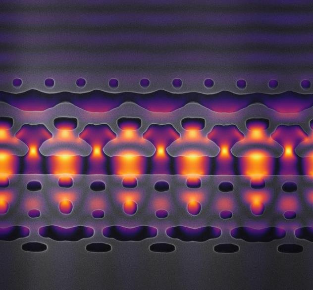
Scientists have developed a new type of particle accelerator that is so small it could fit into a pen tip. The device uses laser light to speed up electrons to velocities of over a hundred thousand kilometres per second. This is the first time that such a tiny accelerator has been able to produce fast and well-focused bunches of electrons that can be used for scientific experiments.
How the device works
The device is made of silicon shaped into thousands of 2-micrometre-tall pillars that are arranged into two parallel lines, each 0.2 millimetres long. This structure is called a photonic crystal waveguide. To run the accelerator, the researchers shine laser light on this pillar-lined “runway” from above while injecting electrons into it from the side. The light waves from the laser interact with the pillars in just the right way to create an electromagnetic field that makes the electrons cluster together in narrow bunches that accelerate through the structure.

Why it is a breakthrough
Particle accelerators are devices that use electric fields and magnets to speed up particles like electrons, protons, or ions. These particles can then be used for various purposes, such as studying the fundamental nature of matter, creating new materials, or treating diseases. However, most particle accelerators are very large and expensive to build and operate. For example, the Large Hadron Collider in Switzerland is 27 kilometres in circumference and costs billions of dollars to run.
The new device is the smallest particle accelerator ever built, and it uses light instead of radio waves to generate electric fields. Light has a much shorter wavelength than radio waves, which means that it can create stronger and more localized fields in a smaller space. This allows the device to accelerate particles faster and more efficiently than conventional accelerators.
What it can do
The device is also the first tiny particle accelerator that can produce fast and well-focused bunches of electrons that can be used for scientific experiments. Previous attempts to miniaturize particle accelerators resulted in either slow or diffuse electron beams that were not very useful. The new device can generate electron beams with energies of up to 0.511 mega-electronvolts, which is comparable to some of the large-scale accelerators. The device can also control the number, shape, and duration of the electron bunches by adjusting the laser parameters.
The researchers say that the device could be used for various applications, such as generating X-rays for imaging, creating ultrafast electron diffraction patterns for studying molecular dynamics, or producing terahertz radiation for spectroscopy. The device could also be integrated with other components on a chip to create more complex systems for particle physics or quantum computing.
How it was developed
The device was developed by a team of researchers from Stanford University, SLAC National Accelerator Laboratory, and the University of California, Los Angeles. The team was led by Jelena Vuckovic, a professor of electrical engineering at Stanford and an expert in nanophotonics. The team used a technique called inverse design to optimize the shape and arrangement of the pillars in the photonic crystal waveguide. Inverse design is a computational method that starts with a desired outcome and then works backwards to find the best way to achieve it.
The team tested the device at SLAC’s Facility for Advanced Accelerator Experimental Tests (FACET), where they used a powerful laser to drive the electrons through the device. They measured the properties of the electron beams using a device called an electron spectrometer. The results showed that the device was able to accelerate electrons faster than ever before in such a small space.
The team published their findings in the journal Science on October 19, 2023.
